Advanced Packaging Market Size, Forecast 2030
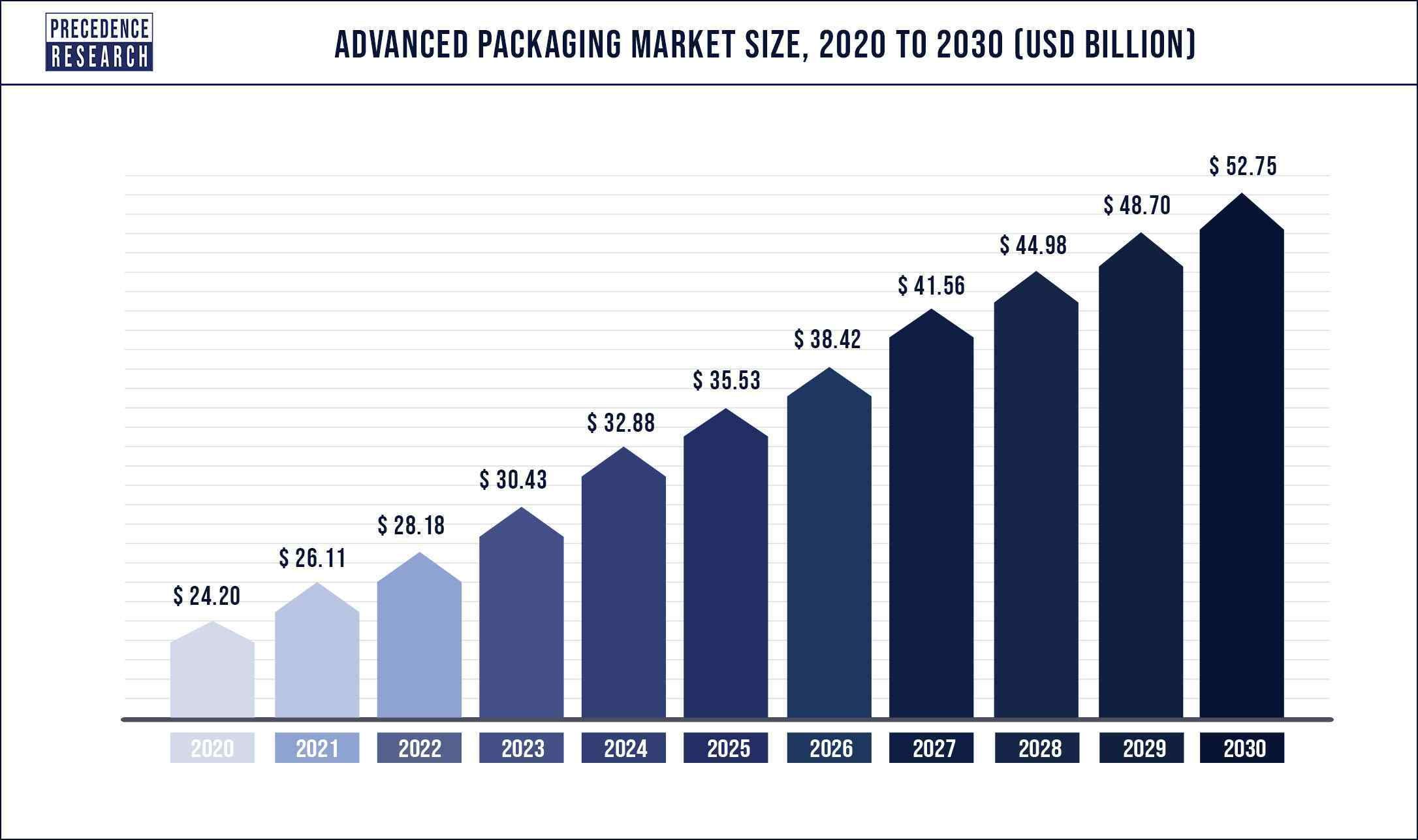
The global advanced packaging market size is projected to reach USD 52.75 billion by 2030 and registering a CAGR of 8.1% from 2022 to 2030
Advanced packaging is a supporting case which prevent from any physical damage or corrosion to silicon wafers, logic units, and memory during the final stage of semiconductor manufacturing procedure. In 2020, The Advanced Packaging Market was valued at US$ 24.2 billion and is expected to grow with a CAGR of 8.1% during the forecast period. It facilitates the chip connection to the circuit board. The advanced packing also involves grouping of a variety of distinct techniques, which include 2.5D, 3D-IC, fan-out-wafer-level packaging, and system-in-package.
Get Report Sample Copy@ https://www.precedenceresearch.com/sample/1337
Regional Snapshots
Asia Pacific leads the advanced packaging market contributing a market share of more than 64% in 2020 and is expected to grow at a CAGR of 8.2% during the forecast period owing to the presence of major market players continuously involved in R&D and in the development of advanced packaging technologies. For instance, on 6th May 2021, Samsung Electronics, a world leader in advanced semiconductor technology, announced the availability of its next-generation 2.5D packaging technology called Interposer-Cube4 (I-Cube4). It is leading the evolution of chip packaging technology. Samsung’s I-Cube, a heterogeneous combination of technologythat uses multiple dies to operate as a single chip in one package by horizontally placing one or more logic dies (CPU, GPU, etc.) and several High Bandwidth Memory (HBM) dies on top of the silicon interposer.
Market Dynamics
Driver - The rise in demand for consumer electronic products across the globe is accelerating the growth of the Advanced Packaging Market. furthermore, the increasing demand for miniaturization of devices is also fostering the market growth.
Restraint - The major restraining factor that will negatively impact the growth of the Advanced Packaging Market includes high cost involved in the design and manufactures of chips at each node and the expensive installation of advanced packaging technology.
Opportunity- The increasing demand for the consumer electronics products in the market and the demand for miniaturization of devices will find huge opportunities that are anticipated to drive the growth of the Advanced Packaging Market.
Challenges - The high installation and manufacturing cost of the advanced packaging is a major challenge encountered by the advanced packaging market and this is expected to hamper the market growth.
Recent Developments
On 11th February 2021, Siemens Digital Industries Software announced that its partnership with Advanced Semiconductor Engineering, Inc. (ASE) has developed two new enablement solutions engineered to help mutual customers create and evaluate multiple complex integrated circuit (IC) package assemblies and interconnect scenarios in an easy-to-use, data-robust graphical environment prior to and during physical design implementation.
On 9th June 2021, NepesCorporationa Korea's top semiconductor back-end process (OSAT) company announced the development of 'nSiP', advanced packaging technology without using the PCBs. NsiP is ased on ‘End-fab’ technology without board and wire bonding and is the most optimized packaging solution for high performance, high density, and small form factor.
In March 2021 Deca, an industry-leading technology provider for advanced semiconductor packaging, has announced the introduction of its new APDK (Adaptive Patterning Design Kit) methodology. This solution is the result of Deca's collaboration with Advanced Semiconductor Engineering Inc. (ASE) and Siemens Digital Industries Software.
In February 2021, Siemens Digital Industries Software announced that the collaboration with Advanced Semiconductor Engineering, Inc. (ASE) developed two new enablement solutions engineered to help mutual customers create and evaluate multiple complex integrated circuit (IC) package assemblies and interconnect scenarios in a data-robust graphical environment prior to and during physical design implementation.
Appreciate the creator